Diode Submounts
Ultra-precise patterning of thin film metals on dielectrics with high thermal conductivity are used for diode submount applications. Via the acquisition of Ion Beam Milling, Inc., SemiGen is the industry leader for laser diode submount fabrication. As each application is different, we work with customers to develop a custom design that perfectly fits their requirements. We have experience producing circuits utilizing substrates of varying thicknesses with high thermal conductivity such as alumina (Al), aluminum nitride (AlN), and beryllium oxide (BeO). SemiGen can deliver laser diode submounts with or without Au/Sn pads depending on your needs.
Diode Submounts
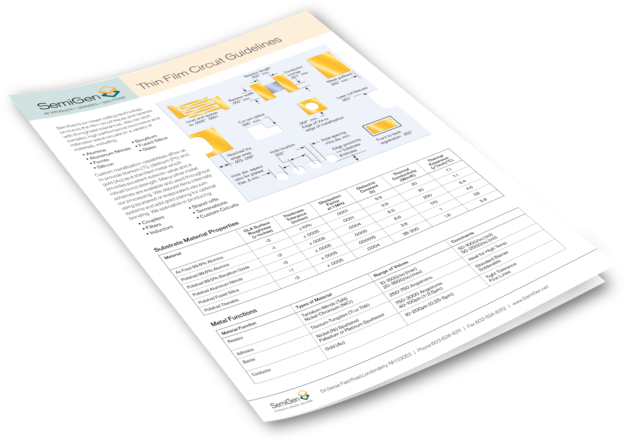
| Dielectric Material |
Thermal Conductivity (w/mk) |
TCE (PPM/°C) |
Dielectric Constant |
Comment |
|---|---|---|---|---|
| Alumina (99.6%) | 26 – 27 | 7.2 | 9.9 | "Good Thermal Compatibility with GaAs-Based Devices" |
| Aluminum Nitride | 170 – 210 | 4.6 | 8.9 | "Good Thermal Compatibility with Si-Based Devices" |
| Beryllium Oxide | 260 – 290 | 8.5 | 6.7 | "Good Thermal Compatibility with GaAs-Based Devices Superior Thermal Performance" |
Standard Submount Metalizations
| Metallization | Thickness | Comments |
|---|---|---|
| Ti/Pt/Au | 1KÅ / 1.5 KÅ / 5KÅ | Best/Universal Choice |
| Ti /Ni/Au | 1KÅ / 1.5 KÅ / 10KÅ Min. | Ni Diffusion above 350 °C |
| Au/Sn (80/20) | 3 to 5 microns | Chip Preform Replacement |
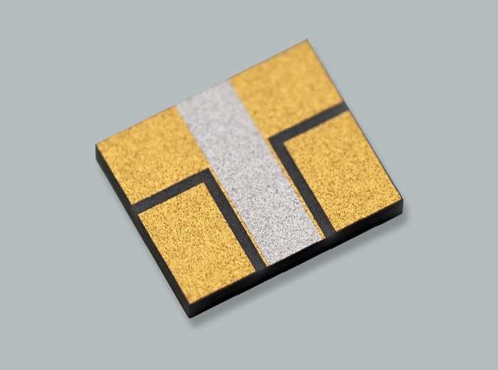
Edge emitting Laser Diodes operating at high current require a heat spreader to be placed between the device active region and the metal carrier package. When arranged in high densities, heat dissipation becomes even more critical. Ultra-precise patterning of thin film metals on dielectrics with high thermal conductivity are used for diode submount applications. Metal pads on the top surface edge of the submount facilitate diode edge mount requirements with edge gap geometrics down to 5 microns.
Au/Sn selective deposition on the Ti/Pt/Au edge pads precludes the need for small solder preforms handling and avoids the risk of potential solder rollup in the critical submount edge areas.
As each application is different, we work with customers to develop a custom design that perfectly fits their requirements. Our team has experience producing circuits utilizing substrates of varying thicknesses with high thermal conductivity such as Alumina, Aluminum Nitride, and Beryllium Oxide.
We can deliver Laser Diode Submounts with or without Au/Sn pads depending on your needs.
Features:
- Metal pads on the top surface edge of the submount facilitate diode edge mount requirements with edge gap geometrics down to 5 microns.
- Au/Sn selective deposition on the Ti/Pt/Au edge pads preclude the need for small solder preforms handling and avoids the risk of potential solder rollup in the critical submount edge areas.
Applications:
Laser diode submounts are employed when edge emitting laser diodes operate at high current and require a heat spreader to be placed between the device active region and the metal carrier package. When arranged in high densities, heat dissipation becomes even more critical.
.png)